Analog & Digital Circuit Trainer: Model No. ADC-17045
Module One: ADC-17045-01
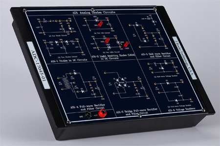
Chapter 1: Analog Diode Circuits
Experiment 1: Diodes in DC Circuits
Experiment 2: Light Emitting Diodes (LEDs) in DC Circuits
Experiment 3: Half-wave Rectifier and Filter Circuit (fin = 50/60 Hz, Vin = 8 ~ 10 Vpp)
Experiment 4: Full-wave Rectifier and Filter Circuit (fin = 50/60 Hz, Vin = 8 ~ 10 Vpp)
Experiment 5: Bridge Rectifier and Filter Circuit (fin = 50/60 Hz, Vin = 8 ~ 10 Vpp)
Experiment 6: Voltage Doublers
Module Two: ADC-17045-02
Chapter 2: Analog Voltage Regulators and Filter Circuits
Experiment 1: Zener Diode as a Voltage Regulator (Vin=12V, Vout = 5V)
Experiment 2: Transistor Series Voltage Regulator ( Vin=12V, Vout = 5V )
Experiment 3: Transistor Shunt Voltage Regulator ( Vin=12V, Vout = 5V)
Experiment 4: Low-pass Filter (Vcc:±12V, Vin: 100Hz ~ 5KHz & 4Vpp)
Experiment 5: High-pass Filter (Vcc:±12V, Vin: 100Hz ~ 5KHz & 4Vpp)
Experiment 6: Bandpass Filter (Vcc:±12V, Vin: 50Hz ~ 280Hz & 4Vpp)
Module Three: ADC-17045-03
Chapter 3: Analog Amplifier and Multivibrator Circuits
Experiment 1: CE Amplifier of NPN Transistor (fin=1~2KHz, Vin=50 ~ 200 mVpp, Vout= 1 ~ 3 Vin)
Experiment 2: CB Amplifier of NPN Transistor(fin=1~2KHz, Vin=50 ~ 200 mVpp, Vout= 6 Vin)
Experiment 3: CC Amplifier of NPN Transistor (fin=1~2KHz, Vin=50 ~ 200 mVpp, Vout= Vin)
Experiment 4: Monostable Multivibrator Using Transistor (Output Frequency: User-Controlled)
Experiment 5: Bistable Multivibrator Using Transistor (Output Frequency: User-Controlled)
Experiment 6: Astable Multivibrator Using Transistor (Output Frequency: 115 kHz)
Module Four: ADC-17045-04
Chapter 4: Basic Logic Gates and Code Conversion Circuits
Experiment 1: Basic Logic Gates Characteristics Measurement
Include Logic Gates: AND Gate; NAND Gate; NOT Gate; OR Gate; NOR Gate; EX-OR (XOR) Gate
Experiment 2: De Morgan’s Law Using Boolean Logic Equation
Experiment 3: Binary to Gray Code Conversion (Binary: 4 bits, Gray Code: 4 bits)
Experiment 4: Gray Code to Binary Conversion (Gray Code: 4 bits, Binary: 4 bits)
Experiment 5: Binary to Excess-3 Code Conversion (Binary: 4 bits, Excess-3 Code: 4 bits)
Experiment 6: Excess-3 Code to Binary Conversion (Excess-3 Code: 4 bits, Binary: 4 bits)
Module Five: ADC-17045-05
Chapter 5: Adder and Subtractor, Comparator, Encoder, and Decoders
Experiment 1: 4 Bits Adder
Digital Input: 4 bits; Data Input Mode: Dip Switch; Output Data Length: 4 bits; Data Display Mode: LED Display
Experiment 2: 4 Bits Subtractor
Digital Input: 4 bits; Data Input Mode: Dip Switch; Output Data Length: 4 bits; Data Display Mode: LED Display
Experiment 3: 4 Bits Comparator
Input Data Length: 4 bits; Data Input Mode: Dip Switch
Output Data Length: 3 bits; Data Display Mode: LED Display
Experiment 4: 8 to 3 Lines Encoder
Input Data Length: 8 bits; Data Input Mode: Dip Switch
Output Data Length: 3 bits; Data Display Mode: LED Display
Experiment 5: 3 to 8 Lines Decoder
Input Data Length: 3 bits; Data Input Mode: Dip Switch
Output Data Length: 8 bits; Data Display Mode: LED Display
Experiment 6: Active-high and Active-low Decoders
Module Six: ADC-17045-06
Chapter 6: Multiplexer and Demultiplexer, Interface Circuits and Parity Generator
Experiment 1: Multiplexer Circuit
Input Data Length: 4 bits; Data Input Mode: Dip Switch
Output Data Length: 1 bit; Data Display Mode: LED Display
Experiment 2: Demultiplexer Circuit
Input Data Length: 1 bit; Data Input Mode: Dip Switch
Output Data Length: 4 bits; Data Display Mode: LED Display
Experiment 3: CMOS and TTL Interface Circuits
TTL to CMOS Transform: Input: 5 V; Output: 12 V
CMOS to TTL Transform: Input: 12 V; Output: 5 V
Experiment 4: Parity Generator Circuit
Input Data Length: 9 bits; Data Input Mode: Dip Switch
Output Data Length: 2 bits; Data Display Mode: LED Display
Experiment 5: To Verify the Dual Nature of Logic Gates
Experiment 6: 7 Segment Driver and Display Circuit
Module Seven: ADC-17045-7
Chapter 7: Clock Generator and Flip-flop Circuits
Experiment 1: Crystal Oscillator Circuit Using Basic Logic and Schmitt Gates
Basic Logic Oscillator: Output Frequency: 3.58 MHz
Schmitt Gates Oscillator: Output Frequency: 3.58 MHz
Experiment 2: 555 IC Astable Multivibrator and Monostable Multivibrator Oscillator Circuit
Astable Multivibrator: 5.25 Hz; Monostable Multivibrator: User Controlled
Experiment 3: RS Flip-flop Circuit
Input Data Length: 2 bits; Data Input Mode: Dip Switch
Output Data Length: 2 bits; Data Display Mode: LED Display
Experiment 4: JK Flip-flop Circuit
Input Data Length: 2 bits; Data Input Mode: Dip Switch
Output Data Length: 2 bits; Data Display Mode: LED Display
Experiment 5: D Flip-flop Circuit
Input Data Length: 1 bit; Data Input Mode: Dip Switch
Output Data Length: 2 bits; Data Display Mode: LED Display
Experiment 6: T Flip-flop Circuit
Input Data Length: 1 bit; Data Input Mode: Dip Switch
Output Data Length: 2 bits; Data Display Mode: LED Display
Module Eight: ADC-17045-08
Chapter 8: Shift Register and Digital Counters
Experiment 1: 4 Bits Shift Register
Input Data Length: 1 bit; Data Input Mode: Dip Switch
Data Display Mode: LED Display
Experiment 2: Johnson Counter
Output Data Length: 4 bits; Data Display Mode: LED Display
Experiment 3: Ring Counter
Experiment 4: Asynchronous Counter
Output Data Length: 4 bits; Data Display Mode: LED Display
Experiment 5: Synchronous Counter
Output Data Length: 5 bits; Data Display Mode: LED Display
Experiment 6: 4 Bits Binary Up and Down Counter
Module Nine: ADC-17045-09
Chapter 9: ADC and DAC, BCD to Decimal Encoder and Decoder
Experiment 1: ADC Circuit
Analog Input: 0 V~5 V; Data Display Mode: LED Display; Resolution: 8 bits
Experiment 2: Unipolar DAC Circuit
Digital Input: 8 bits; Data Input Mode: Dip Switch; Analog Output:0 V ~ 5 V; Step Value: 0.019 V
Experiment 3: Bipolar DAC Circuit
Digital Input: 8 bits; Data Input Mode: Dip Switch; Analog Output:-5 V ~ 5 V; Step Value: 0.038 V
Experiment 4: BCD to Decimal Decoder
Experiment 5: BCD Priority Encoder
Experiment 6: Pulse Stretcher Circuit